Introduction:
In the past, EMC compatibility has been a module-level or system-level issue for electronics.
Electronic equipment manufacturers are now beginning to require semiconductor manufacturers to specify emission and immunity levels for integrated circuits (ICs). Some semiconductor companies have responded by developing proprietary test methods, while others have worked with equipment manufacturers and the International Electrotechnical Commission (IEC) to develop some general-purpose standardized methods for IC EMC test and measurement. That's why understanding IC EMC integrated circuit EMC test systems has become especially important for chip designers.
IC EMC Problem Sources:
In addition to wiring and structural design, the characteristics of the IC used in the device also determine its EMC characteristics. the sensitivity of the IC to fast pulses increases significantly with its structure size, operating voltage, and fewer operating points. The current field of IC and microcontroller development is converging towards structures smaller than 100nm, and even computer chipsets have reached 7nm, and the accompanying higher switching rates have resulted in a decrease in the EMC-EMS immunity of ICs compared to earlier products by nearly 90%. This trend will ultimately be reflected in the EMC characteristics of the device level. Therefore, for ICs with the same functionality, good EMC characteristics can increase the competitive advantage of IC manufacturers.More on IC EMC Problem Sources
How to improve the EMC compatibility competitiveness of ICs?
Improving the EMC performance of IC integrated circuits should start with compliance with IEC standards:
In the absence of the appropriate capabilities and qualifications to plan EMC standards for their own products, IC manufacturers should first follow the International Electrotechnical Commission's IEC test standards. Then they should utilize the IEC standards to develop their own corporate standards for their products.
Now, IEC Technical Committee TC 47 (Semiconductor Devices) is leading the IEC's work. The committee assigned work on the EMC measurement standard to its subcommittee (SC) 47A+ Integrated Circuits.TC 47/SC 47A created Working Group (WG) 9 to prepare test and measurement methods.The WG9 work program cooperates with other industry and national standards bodies such as the Society of Automotive Engineers (SAE) and VDE (VDE) of Germany. (VDE) in Germany. Like the EMC standards at the product and equipment level, IC-EMC includes a family of standards for two tests, RF EMI and RF Immunity EMS.
- For a list of the latest IC EMC test standards, please click here:What are the EMC test standards for IC integrated circuits?
- For detailed IC emc test items, please check:IC EMC Test Equipment and Test Methods
Create a Realistic EMC Environment with IC EMC Integrated Circuit EMC Test Systems
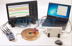
With 深圳市易优特测试技术有限公司's German langer-emv IC test system, users can create a realistic EMC environment during the development process by injecting pulses of various parameters, so that IC circuit designers can easily see the effects of IC on various types of interference and improve the chip design. This allows IC circuit designers to easily see the impact of ICs on various types of interference and improve the design of the chip.The IC test system can adequately protect the sensitive and fragile pins on the IC during testing.
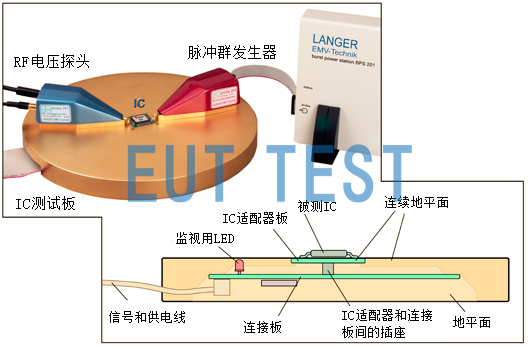
Injection of pulse interference into IC test systems using langer-emv for ICs
Using the new IC EMC test system:
Using the new IC EMC test system provided by EUTTEST (Figure 1respond in singingFigure 2) can be used to analyze the behavior of ICs under the selective influence of interference (conducted and radiated) and/or corresponding emissions. The insights gained from this analysis help semiconductor manufacturers to optimize ICs and IC users to overcome weaknesses in their electronic modules. Note: The IC chip under test must be operational and its operating status should be determined by oscilloscope, sending packets, etc. before starting the test.
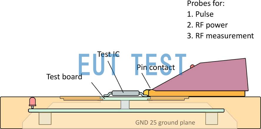
Fig. 1 Fundamentals of measurements using the IC test system (conduction)
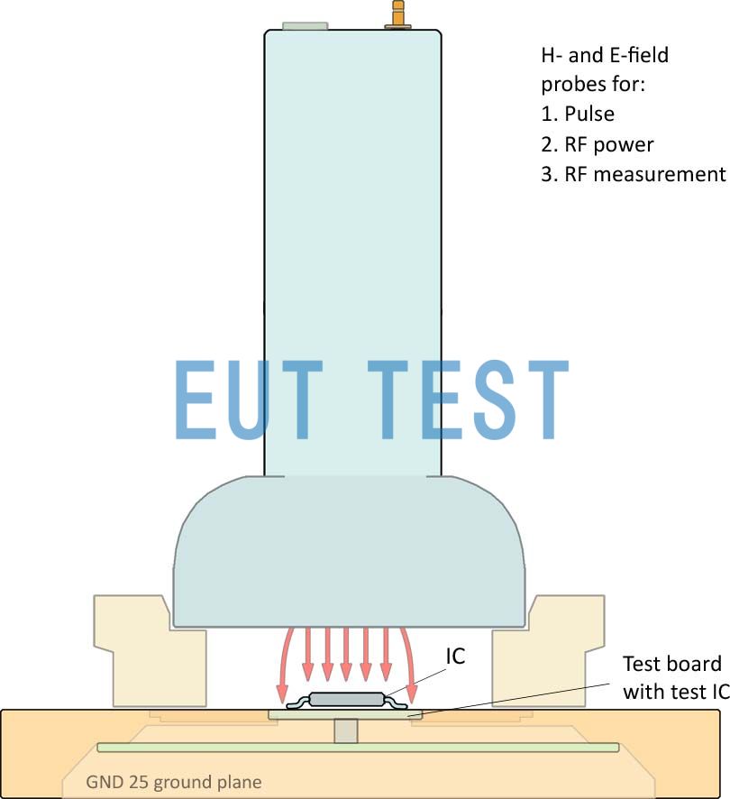
Fig. 2 Basic principle of measurement using IC test system (radiation)
Benefits of EMC testing for ICs:
IC test systems allow IC users:
- Identifying EMC Issues in Devices at the IC Level
- Based on the insights gained, select the IC and
- Optimize the circuit and/or layout design based on the EMV parameters of the IC.
IC test systems allow IC manufacturers to:
- Measuring and checking the immunity/radiation of ICs
- Determining Causes of Interference and Optimizing IC EMC Issues
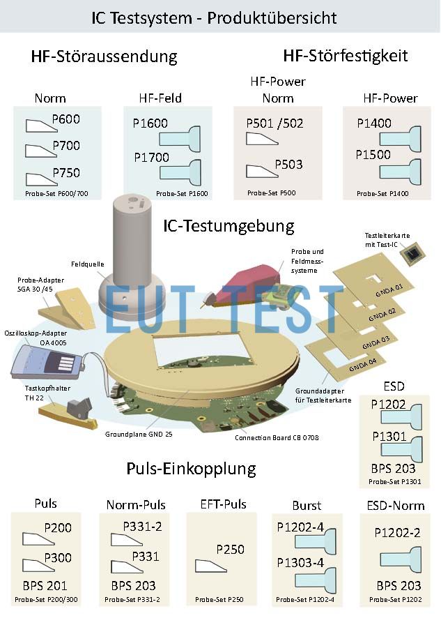
Fig. 3 Overview of IC test system with measurement system/probe set for ICE1 IC test environment
EMC Parameters for ICs.
- Each IC has characteristic immunities associated with conducted and radiated interference. these are its EMC parameters. These are its EMC parameters. the IC pins have conducted immunity that can be measured using the appropriate probes in the probe set.
- The entire IC is radiated immunity. Interference fields can affect the IC externally and exceed these immunity levels to magnetic and electric fields. These immunity levels are independent of each other. A probe that generates a suitable and defined field is required to determine the level of field immunity.
- In addition, the conducted interference emissions of the IC can be measured via the pins and the radiated (electrical and magnetic near-field) emissions can be measured via the IC housing. The measured curves can be used to analyze the EMC parameters of the IC.
IC test system setup.
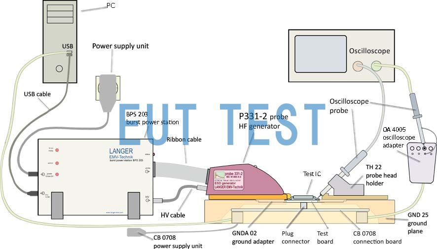
Figure 4 Cross-section of ICE1 IC test environment with probe and test IC (performed)
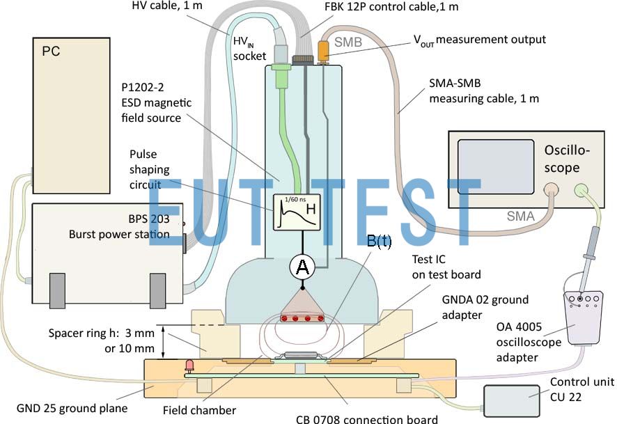
Figure 5 Profile of ICE1 IC test environment with probe and test IC (radiation)
The IC under test is located on a test board in the test setup. A filtered connection links the test board to a connection plate located below it, which connects the test IC to a PC. the IC can be controlled and monitored using the supplied software. the connection plate is located on the lower side of the ground plane, forming a fixed ground reference system for measurements. the probe is placed on the ground plane to inject interference into the test IC or to measure its emission through conductive or capacitive/inductive coupling. The probe is placed on the ground plane and is used to inject interference into the test IC or to measure its emission through conductive or capacitive/inductive coupling. The measurement connection is made by the probe's pins touching the measured pins of the test IC. This small setup and the continuous ground plane ensure that measurements can also be performed in the GHz range.
IC EMC Test Methods.
We can now use IC EMC test equipment to conduct tests according to the test methods defined in the standard, it is important to note that the EMC tester must analyze the EMC immunity and emission mechanisms in the device, all interference variables (RF, ESD, EFT, emission, RF emission ......) test methods are derived from this analysis. .
IC EMC immunity test
Test methods for devices generate electric and magnetic fields in the device under test. These fields affect the network of printed circuit boards leading to the IC and the IC housing. The fields acting on the networks generate currents and voltages in these networks that affect the connected ICs.
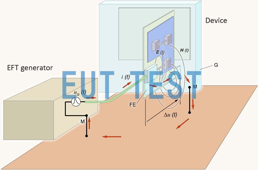
Figure 6 EFT Test Bench
The IC's test generator typically must simulate these electrical and magnetic parameters.Figure 6Shows the basic setup of the burst or ESD test bench. Injecting the Device Under Test u G The test pulse at (t) generates a current pulse i(t) that flows through the device. This causes a voltage drop in the device D u (t). This voltage drop D u (t) generates an electric field strength E(t) in the device. The current i(t) generates a pulsed magnetic field H(t) in the device. These fields have an indirect effect on the externally connected conductor tracks on the IC (conduction) or directly on the IC housing (radiation).
IC EMC Interference Emission Test
Switch-mode ICs generate internal RF currents and voltages. These, in turn, generate electric or magnetic RF fields that escape directly from the IC case. In addition, RF voltages and currents can be transmitted to the IC pins and therefore to networks external to the IC on the printed circuit board where they generate RF and/or RF fields. The electric field E is determined by theIn Figure 7of the IC and the external network of the IC generates. The electric field couples to the neighboring component and stimulates it to emit interference. In this case, the EMC parameters of the IC are the strength of the electric field emitted by the IC and the electrical parameters current and voltage (IC emission) of the external network of the IC that is stimulated.
A suitable system (probe set) must be used to measure the electric and magnetic field parameters of the IC case as well as the RF currents and voltages of the IC pins. These are characteristics of the IC.
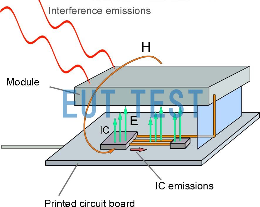
Fig. 7 Stimulation of interference emission in an electronic device by an electric field through an IC and a network of printed circuit boards
IC EMC Magnetic/Inductive Coupling Testing
The pulsed interference currents flowing through the board generate pulsed magnetic fields. These magnetic fields B Stcan be coupled into the conductor loop and induce an interference voltage u St. Pulsed magnetic fields can interfere with the function of the IC in two ways (Figure 8):
The induced voltage affects the IC pins that are switched as inputs. The disturbance voltage uSt is converted to a spurious signal in the IC by the input circuitry and further processed into a logic signal.
The induced voltage drives the interference current i Stpins into the IC. If these are Vdd/Vss pins, this interference current goes directly into the IC's internal Vdd/Vss system. However, it can also enter through the signal pins and be directed to the IC's internal Vdd/Vss system via internal drivers or protection diodes or capacitors. the Vdd/Vss system passes the interference current to other functional components of the IC, so that failures may occur in areas that are not functionally connected to the affected pins.
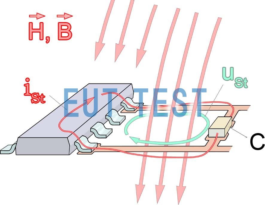
Fig. 8 IC interference caused by pulsed magnetic field
IC EMC Electrical/Capacitive Coupling Testing
The module may be exposed to several pulsed electric fields of 10,000 V/m (test setup according to IEC 61000-4-4), which can also affect the board network (Figure 9). The displacement current D flows around through the parasitic capacitance of the line. ICs connected to the line are affected in two ways:
The network essentially has circuit elements R, L and diodes for Vdd and Vss on the board and in the IC. The displacement currents generate interference pulses on these elements u St. This interference pulse is converted into a parasitic signal in the IC by the input circuitry and is further processed as a logic signal.
The displacement current is split into two parts. The first part is discharged through the equivalent circuit of the board and any decoupling capacitors that may be present. The second part of the disturbance current i StIt flows through the IC via the driver or protection diode to the Vdd/Vss system. It produces an effect similar to magnetic coupling.
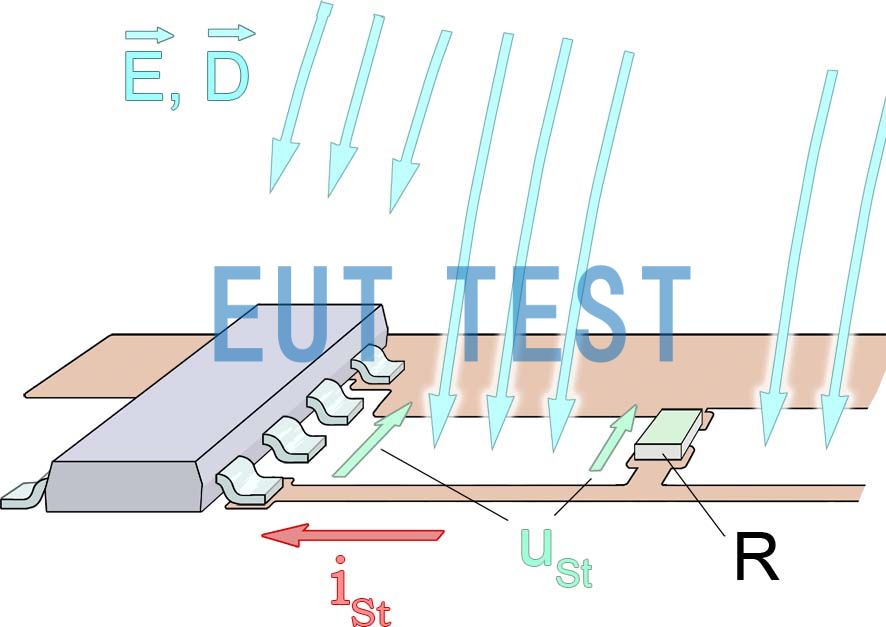
Fig. 9 Pulsed Magnetic Field Interference with IC

