
EMC Test Analysis from Device to Chip - Part 1
present (sb for a job etc)
Compliance with EMC requirements is becoming increasingly demanding. While technological advances have allowed for the reduction of feature sizes, this has led to special challenges in the immunity of control equipment.
These increased requirements for immunity add significant costs to the development and manufacture of devices. However, by testing immunity at the component level (i.e., ASICs and ICs), countermeasures can be more easily identified and taken. These immunity test results allow pre-selection of specific ICs and ASICs for further module development. In addition, they can be incorporated into IC and ASIC development and contribute to component optimization.
While there are test procedures in the industry that provide extensive experience in evaluating IC and ASIC immunity, the concept behind current test methods is to apply interference pulses directly to the pins of the test IC. The shape and amplitude of the applied disturbance is specifically chosen to simulate the typical disturbances that the IC will experience when the device it is in is subjected to standardized immunity testing or in a disturbed environment.
During operation, technical equipment, facilities and installations are generally powered by impulsive interference signals. Standard equipment tests therefore simulate, for example, spark generation (bursts) or electrostatic discharges (ESD) at switch contacts.
Using standard test methods, it is possible to observe the immunity in active mode (i.e., the behavior of a voltage-supplied IC in normal operation). The criterion for passing the test is that the function is not disturbed.
Environmental influences or the test itself may cause voltages and currents to be significantly higher than the specified maximum values of the IC.
However, the advantage of analyzing immunity at the IC level is that it is not necessary to take into account the impact of equipment design on EMC. This includes, for example, the design of the printed circuit board, the nature and availability of the connectors or the enclosure construction.
In addition, when testing IC immunity, interference effects are not as pronounced as when testing the [entire] device. This results in better reproducibility of test results. This document describes the link between device testing and IC pin testing.
Equipment Testing
Due to the increasing digitization and widespread use of electronic products and the high demands placed on the robustness of equipment immunity, it is particularly important to carry out immunity tests for pulsed disturbances when testing technical facilities and equipment. This is because they are also subject to pulse-like disturbances during operation and standard use.
The following standards describe the disturbing impulses (bursts and ESD) relevant for immunity testing: IEC 61000-4-4 Fast Transient Immunity Testing (bursts) and IEC 61000-4-2 Electrostatic Discharge Immunity (ESD):
| IEC 61000-4-4 | Fast transient immunity test (burst) |
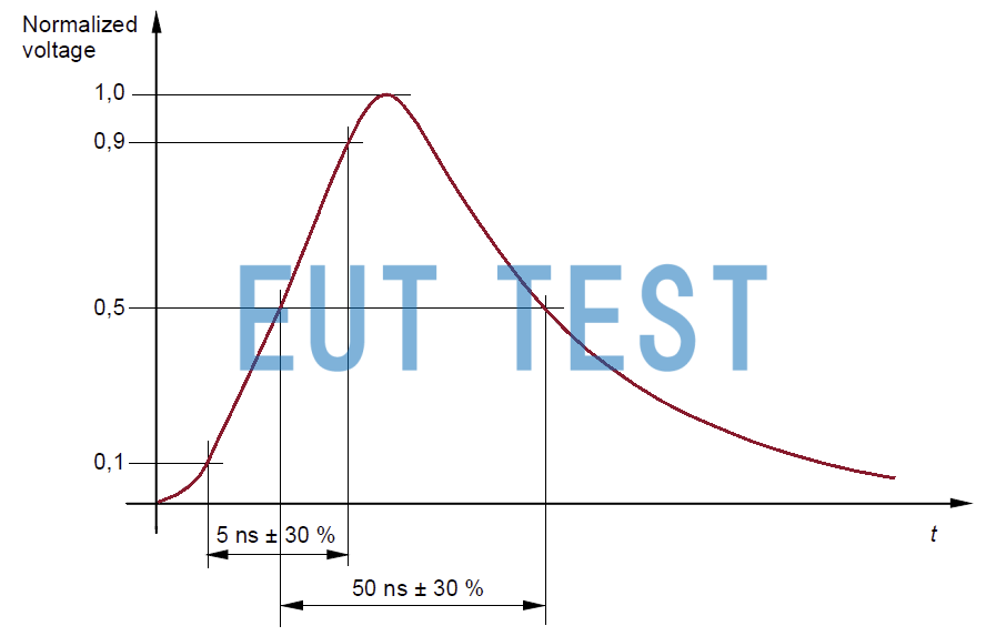 Fig. 1 Time profile of bursts according to IEC 61000-4-4 | |
A pulse with a source impedance of 50 ohms is applied to the device from a minimum of ±2 kV with a leading edge of 5 ns and a trailing edge of 50 ns (half amplitude) (Figure 1). It is from these pulses that the burst is composed.
<<<<提醒:左右滑动表格>>>>| IEC 61000-4-2 | Electrostatic Discharge Immunity Test (ESD) |
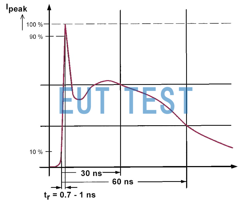 Figure 2 ESD Pulse Time Curve according to IEC 61000-4-2 | |
Pulses with a source impedance of 330 ohms are at least ±6 kV, with a leading edge of 0.7 ns and a trailing edge of 5 ns (half amplitude) (Figure 2)
EMC Test Analysis from Device to Chip - Fundamentals of Device Test Interference
To demonstrate its immunity, pulse-shaped disturbances are applied to and independent of the intended location of the device. A primary disturbance pulse (ESD or burst) of voltage u(t) applied to the device causes a pulsed disturbance current i(t) to flow through the device (Figure 3). The two basic mechanisms - magnetic coupling and electric (E-field) coupling - should be considered separately, although they occur simultaneously.
1. Magnetic field (inductive) coupling
Magnetic field interference H(t) forms around a conductor carrying an interference current i(t). The lower the impedance of the primary circuit, the higher the current and therefore the higher the magnetic field.
In the ideal case, the field strength of a straight conductor is given by the following equation:
| [1] | 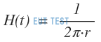 |
Magnetic field interference can penetrate the device and surrounding components and printed circuit boards. Conductor loops are located on the printed circuit board or in components (e.g., ICs thatFigure 3). The magnetic field disturbance induces a secondary disturbance voltage u_sec(t) through the inductor L. The magnetic field interference is not caused by the inductor.
<<<<提醒:左右滑动表格>>>>| [2] | 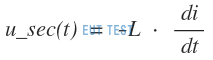 |
For example, such disturbing voltages may be present on or in the IC pic, which may cause the IC to malfunction.
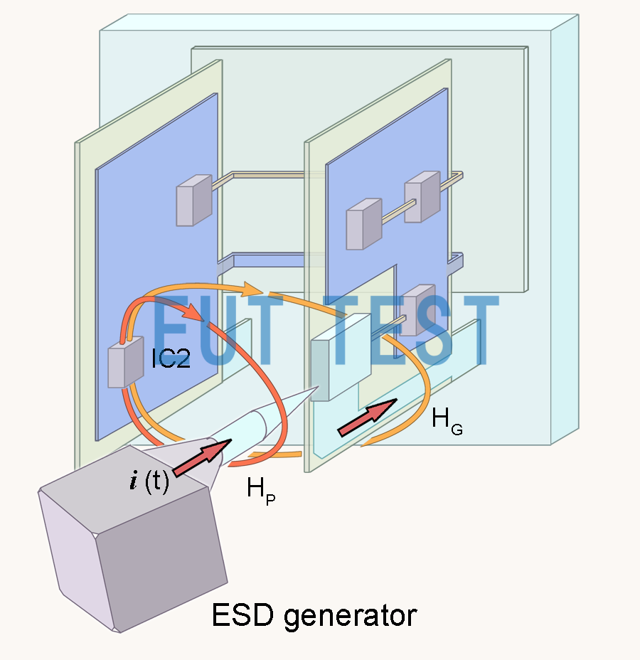
Fig. 3 Mechanism of magnetic field coupling in electrical equipment
2. Electric field coupling
A major disturbance pulse (ESD or burst) of voltage u(t) applied to the device causes a voltage drop across the assembly ((Figure 4)). The electric field E(t) is obtained from the voltage difference along the observed geometry. The higher the impedance of the primary current path, the higher the voltage difference and therefore the higher the resulting electric field. The electric field transfers the disturbance as a displacement current i(t) via capacitive coupling into the secondary circuit, e.g. [at] signal cables and/or IC pins. This process can be realized with a coupling capacitance C in the fF range, as described in [3] below. The capacitively coupled current i(t) generates an interfering voltage at the internal resistance of the secondary circuit. This disturbance voltage may appear on the IC pin and trigger a disturbance in the IC.
<<<<提醒:左右滑动表格>>>>| [3] | 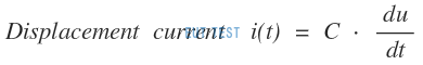 |
Fig. 4 Mechanisms of electric field coupling in electrical equipment
In both cases (coupling due to magnetic or E-field), the interference is reduced by a factor (device factor) during the transition from the primary interference circuit to the secondary circuit and is located in the active electronic device (e.g., on the IC). The 6 kV interference voltage that typically occurs during ESD device testing is reduced to a range of ...0.1 V to several hundred V. This reduction depends on the primary and secondary interference circuits. This reduction depends on the impedance in the primary and secondary interference circuits.
ICs mounted on printed circuit boards are exposed to interference-driven magnetic fields H(t) and E fields E(t).
Magnetic field (inductively) coupled to IC
Magnetic flux density B st (t) across the smallest conductor loop (e.g., between the IC and the connected decoupling capacitor.Figure 5). As described in [4] and [5], the magnetic flux Φ induces in the circuit loop a voltage U stThe
<<<<提醒:左右滑动表格>>>>| [4] |
| [5] |  |
Voltage U stThis source of interference has a low impedance due to its formation in the conductor loop. This results in a high current I st (t).
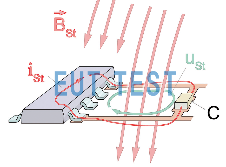
Fig. 5 Model of coupling to IC through magnetic field
EMC Test Analysis from Device to Chip - Electric Field (Capacitive) Coupling to ICs
The electric field strength E(t) or the displacement current D(t) associated with a conducting surface produces interference in the conductor I st (t) (Figure 6). This interference leads to an increase in the voltage on the conducting surface U st (t). This voltage rise distorts the logic signals transmitted through the alignment. The displacement current I st (t) can also be incorporated into the IC and trigger further interference events. The "electric field" source has a high impedance.
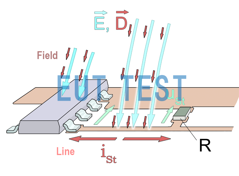
Fig. 6 Model coupled to IC through E-field
analog (device, as opposed digital)
The following simulations (Figure 7-12) demonstrates the general situation. InFigure 7The generation of ESD pulses has been greatly simplified. The equivalent circuit is based on theFigure 4centeras shownThe principle of capacitive coupling.
Estimating Interference Voltage on IC
Positive interference pulses with an amplitude of 6kV are injected into the primary interference circuit as contact discharges (Figure 7The peak interference voltage of 1.4 kV (U st ) is derived from the primary impedance R1 (Figure 4). the 13.5 V interference voltage is kept in contact with the high impedance IC pins by capacitive coupling (electric field coupling) across C1. The impedance of the primary interference circuit can be much larger (1kOhm), allowing the interference voltage at the IC pin to exceed 100 V. This permits significant exceedance of the IC's maximum rating specification.
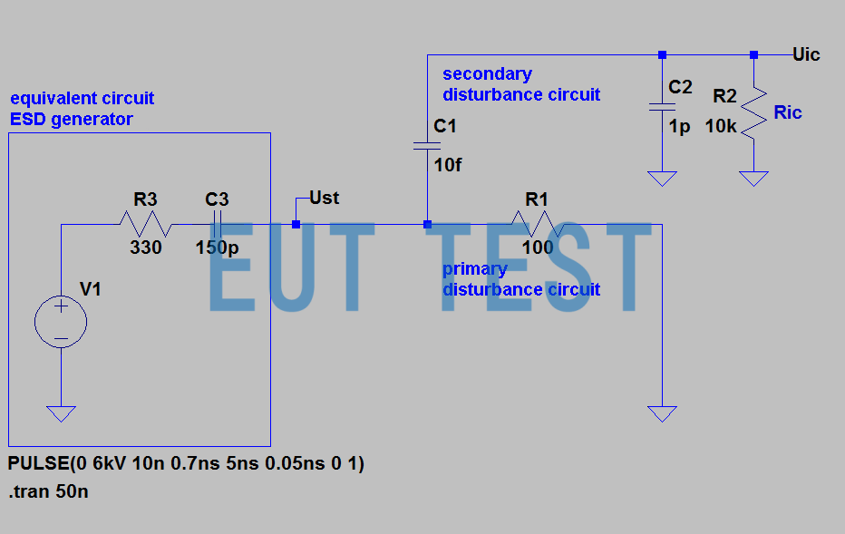
Figure 7 Example of Estimating Interference Voltage on IC Pin when Coupling Electrical Interference Field
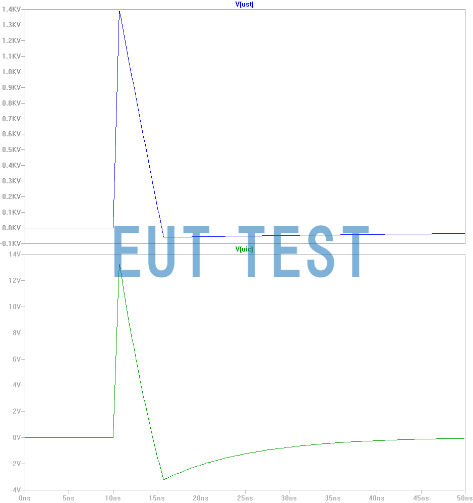
Fig. 8 Coupled interference voltage curves and peak values of primary and secondary circuits
coupling method
The type of coupling also depends on the ratio of the source impedance to the load impedance, i.e. to the input impedance of the IC.
Electric field (capacitive) coupling
The slope is 1 ns and the maximum rate of transmission is 1 GHz. assume that the coupling capacitor C1 is 1 pF. the impedance X of the coupling capacitor is 159 ohms. When the input resistance of IC is 10k, the input resistance is much larger than the source resistance (impedance of C1). As a result, the neighboring interference pulse at R2 (at IC) has the same waveform as the main interference pulse. This results in a proportional voltage divider to the capacitive divider C1 and C2.
IC's Ri ≫ X C1
Completely different conditions are obtained when the load impedance is less than the source impedance. The following example assumes R2 = 100 and C1 = 10fF.
Ri < X for IC C1
Under these conditions, the main interference pulses are distinguished at the IC (Figure 9respond in singing10).

Fig. 9 Equivalent circuit of differential effect of interference coupling through electric field
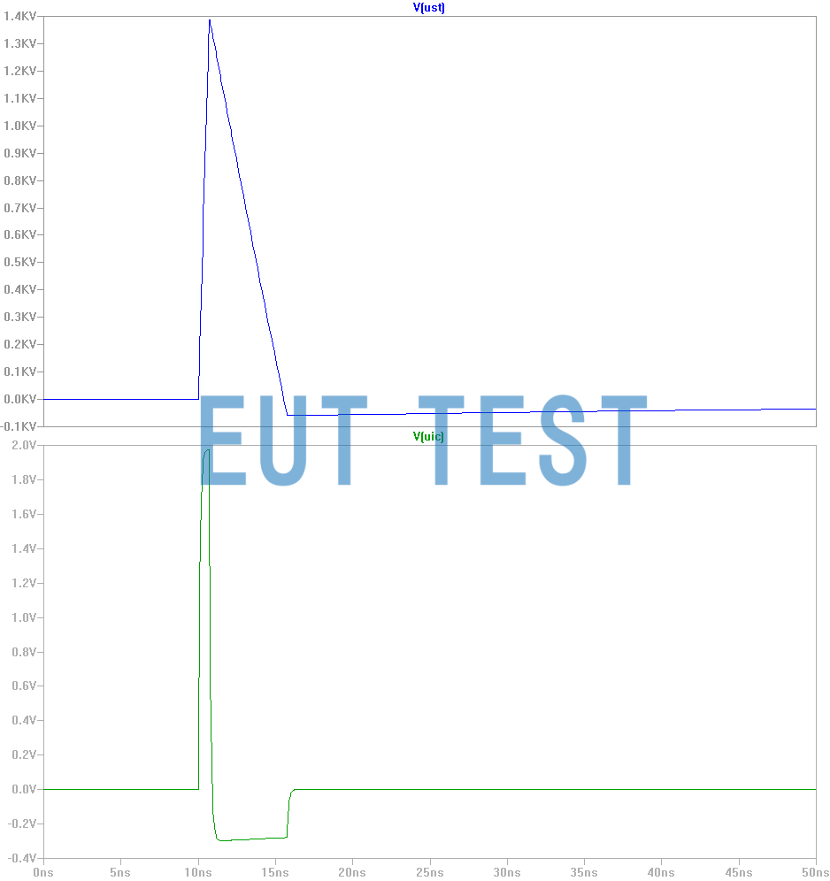
Fig. 10 Differential effect curve of electric field interference coupling
Magnetic field (magnetic) coupling
For H-field coupling, the conditions are reversed. In the idle state, the
R ic ≫ X ss is differential.
R ic < X ssIt's triage.
Summary of the coupling mechanismAs shown in Figure 11Shown. In magnetic coupling, it is assumed that the transformer equivalent circuit diagram has a main inductance (L h ) and leakage inductance (L s ).
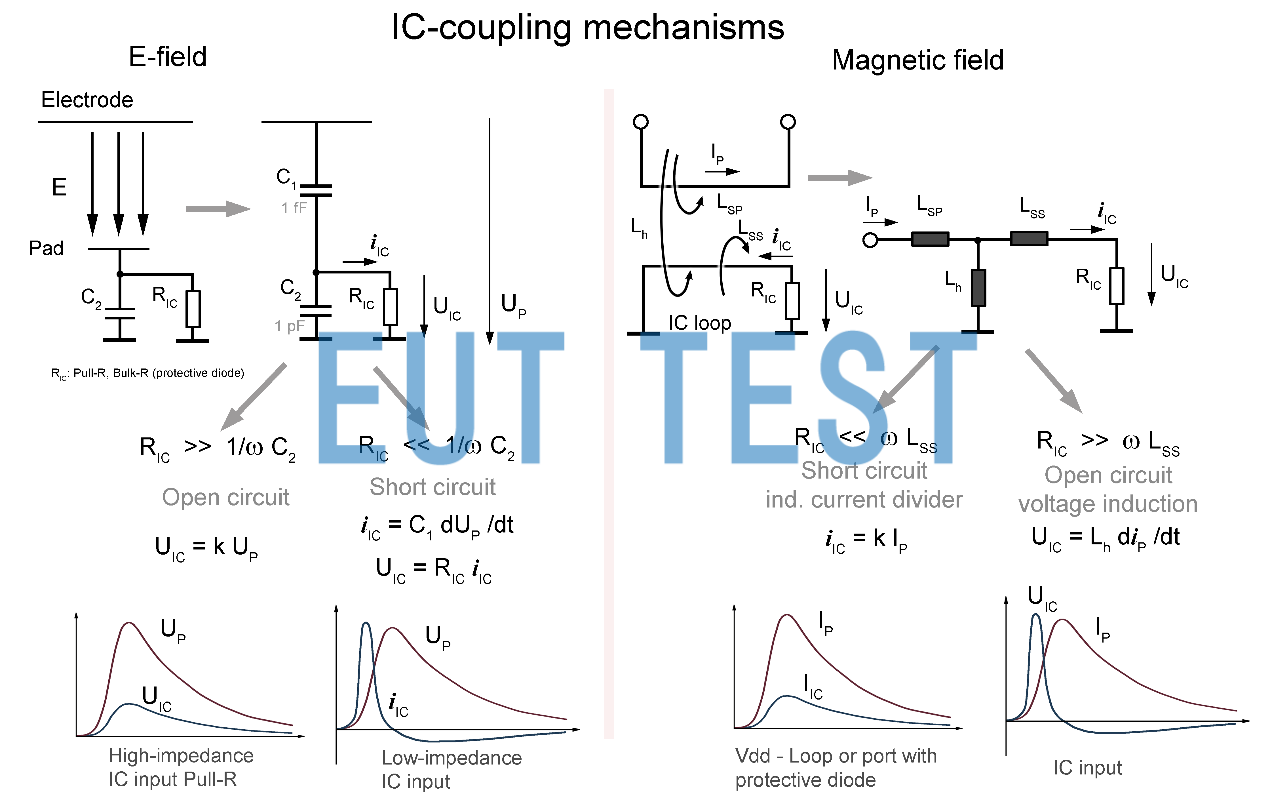
Fig. 11 Operating region of the IC coupling mechanism: current-voltage-divider/differential
EMC Test Analysis from Device to Chip - Part 2
Integrated Circuit Effects
Protection mechanisms are integrated into the IC to prevent surges from damaging its sensitive structures.
Due to the way these existing protection systems are designed, it is assumed that the IC to be protected is not powered by the supply voltage, i.e. it does not operate. As a result, the IC is protected from high electrostatic voltages, which can result in occurrences during the manufacture, transportation and processing of electronic equipment.
In contrast to existing IC protection system designs, the ICs in the above device tests are powered by the supply voltage and are therefore in an operational state.
The protection circuit may inadvertently cause an internal short circuit when disturbed during actual operation (IC power supply).
Protection mechanisms integrated into ICs are not typically disclosed by the manufacturer. However, the following mechanisms can be assumed:
- Surge at the power connection is limited by the structure that functionally corresponds to the Z diode.
- Input and output overvoltage is limited by diode or transistor construction.
The load impedance depends on the IC pin to be tested. The power connections are characterized by low load impedance. At these connections, capacitively coupled signals are differentiated as described above. If the signal is inductively coupled, the voltage will be split. The impedance of the IC inputs will be relatively high when the limiting voltage of the protection circuit is kept within the specified level range. If this range is exceeded, a capacitively bridged power system will result in a sharp decrease in the impedance of the protection circuit and the power supply.
This results in a combination of voltage-sharing behavior and differences in the voltage limiting effect of the protection element. An internal function error is triggered when disturbing currents flow into the IC through the protection circuit.
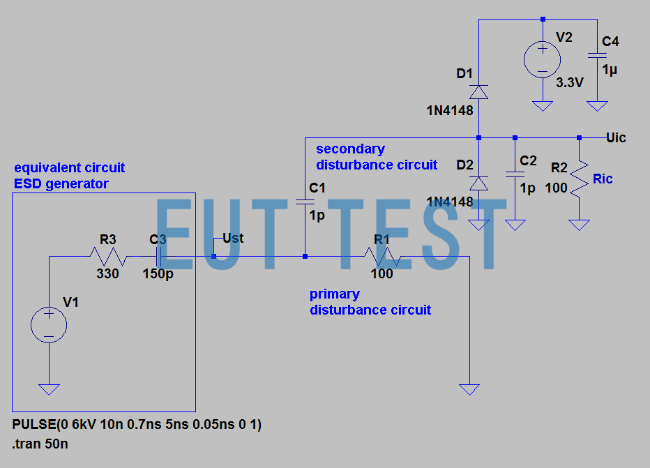
Figure 1 Simplified equivalent circuit of an ESD gun with integrated IC inputs. Input with protection diode
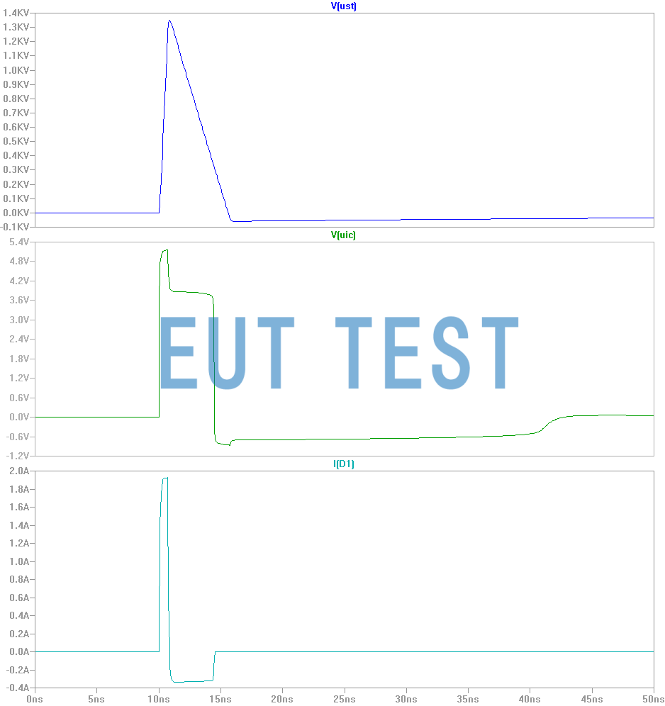
Fig. 2 Interference voltage profile of Fig. 1
Figure 2 Figure 1Interference Voltage Curve
Depending on the characteristics of the diode, different curve trajectories occur.Figure 1respond in singingFigure 2A slow Si diode is used.
The significant disturbance current I(D1) flowing through the diode into the power supply system is obvious. This can be seen in theIn Figure 2See. It is important to consider that this occurs not only during device testing (according to IEC 61000-4-2), but also during normal application of the IC where the electrostatic discharge occurs.
Pulse width required for IC testing
The purpose of defining test pulses for IC immunity testing is to be able to repeat the test of an IC over a wide range of structural widths.This is because the internal processing speed of an IC depends on its structural width. For example, a coarse structure IC has some inertia to disturbing events.
Dynamic switching thresholds/interference thresholds can be used as a basis for evaluating the IC.
Figure 3The pulse width T of the perturbation pulse on the X-axis and the perturbation threshold on the Y-axis are shown. For wide pulses (Figure 3, > 1.5 ns), the interference threshold is close to constant (static interference threshold). For short pulses (Figure 3, < 1.5 ns), the interference threshold increases and the IC becomes insensitive (dynamic interference threshold). The boundary of the static/dynamic transition depends on the structural width of the IC.
In the case of power system disturbances, additional behavioral patterns should be considered. As in the case of determining theIn Figure 3The pulse width of the test generator used to test the IC must be > 1.5 ns. Due to the push for better and faster technology, this limit is variable, allowing faster ICs with pulse widths < 1.5 ns.
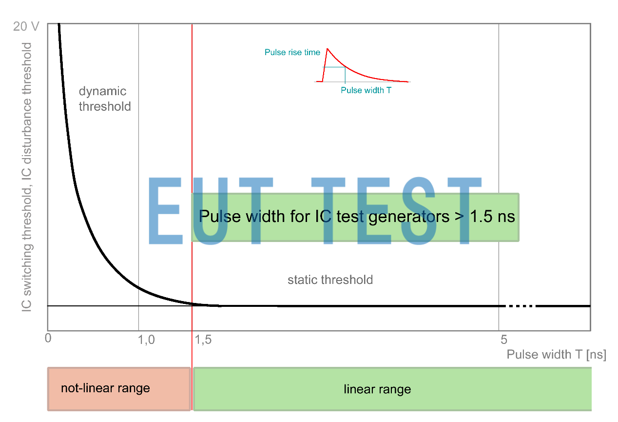
Fig. 3 Describes the static and dynamic interference thresholds for ICs
In order to obtain reproducible results, the pulse width of the IC test must be selected within the linear range (i.e., within the static disturbance interference threshold).
Twenty years ago, ICs with interference pulses of 2 ns could not be disturbed. As technology advances, the structure width decreases and the shift from static to dynamic range moves to shorter pulse widths.
As a result, today's test pulses in the static range can also be used for ICs in faster and future technologies.
Conversely, however, it is important to note that ICs with smaller structures and lower supply voltages have lower interference thresholds and higher sensitivity. As a result, the importance of immunity testing will only increase in the future.
IC Test Methods
Based on preliminary considerations, both low-impedance and high-impedance pulse sources should be available. The following factors should be considered: replacement circuits, edge steepness and maximum voltage level.
The Low Impedance Pulse Source (Probe P2xx) is used to test the power connections. To do this, the support capacitor is removed from the circuit to be tested. It is replaced by the C PCapacitors are replaced. the pulse width of the Probe P2xx is formed by the leading and trailing edges and is 1.2 ns/3.5 ns over the static interference threshold.
Low Impedance Pulse Source (Low Impedance Probe P2xx)
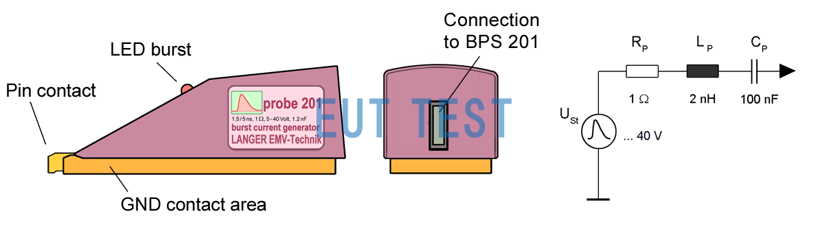
Fig. 4 Structure and equivalent circuit diagram of the low impedance probe
| R P = 1 Ohm |
| L P ≤ 2 nH |
| Ç P ≥100 nF |
| Voltage up to approx. ± 40 volts |
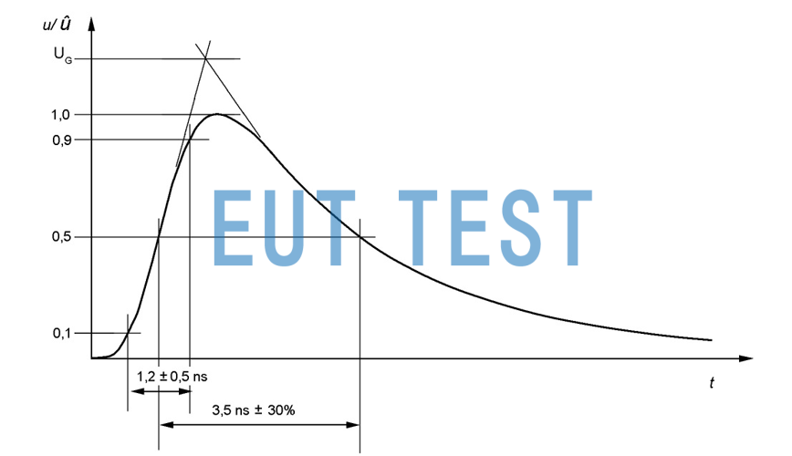
Fig. 5 Curve shape of low impedance probe
High Impedance Pulse Source (High Impedance Probe P3xx)
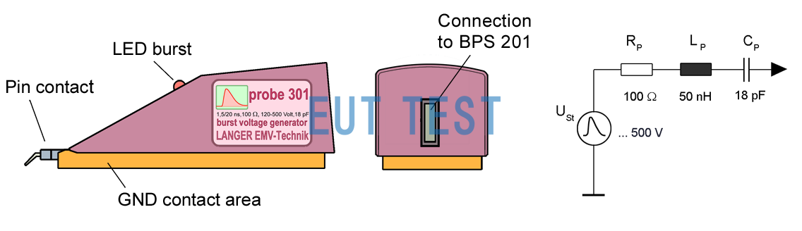
Fig. 6 Structure and equivalent circuit of high impedance probe
| R P = 100 Ohm |
| L P ≤ 50 nH |
| Ç P = 18 pF |
| Voltage up to approx. ± 500 volts |
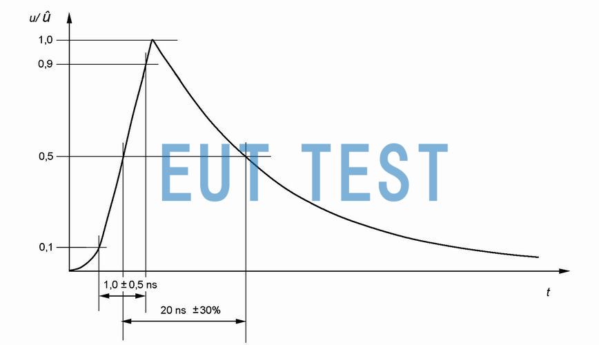
Fig. 7 Curve shape of high impedance probe
The pulse width of the Probe 3xx is formed by the leading and trailing edges and is 1 ns/20 ns within the static interference threshold.If a short circuit occurs, the pulse width of the Probe P3xx decreases to 2 ns.This occurs when the protection circuit is energized to re-establish the pulse width within the static interference threshold. Internal transient processes further amplify the interference pulse.
Figure 8The pin interference thresholds of the IC are shown at the granularity level.
Particularly vulnerable pins can be identified with some comparative experience. Exposed pins should be able to withstand > ±15 V for low impedance source interference thresholds and > ±150 V for high impedance source interference thresholds.
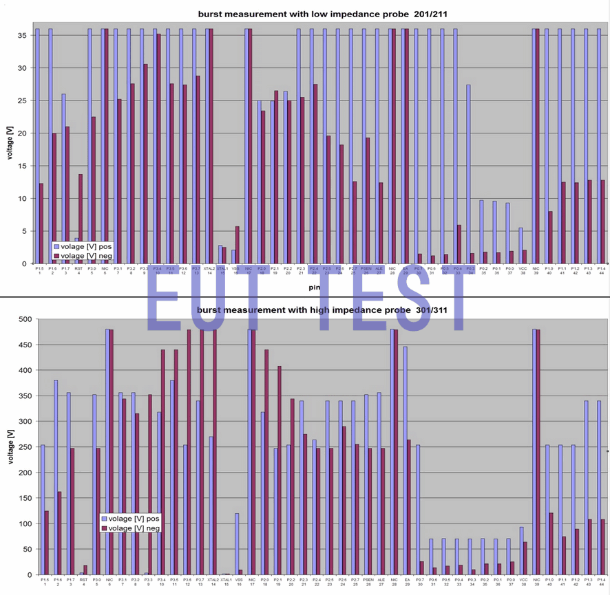
Figure 8 8051 IC Pin Granularity Interference Thresholds
Figure 8 8051 IC Pin Granularity Interference Thresholds
Simulation using IC test pulses
In order to evaluate the impact of the described test pulses, a test pulse simulation model can be used.
This helps the manufacturer of the IC or ASIC to predict the results of the proposed test method. It is worth noting what happens inside the IC during an interference; which circuits are affected and how. Internal parasitic components, such as line inductance and parasitic capacitance, as well as the actual protection structure, which is known only to the IC manufacturer, play a crucial role.
In addition to signal distortion, disturbances in the internal power supply system play a decisive role in fault analysis. External signal distortions can generally be controlled by design measures such as telegraphic repetition and error correction. However, if interference events cause partial internal power supply crashes or oscillations, they cannot be controlled. This can affect the overall functionality of the IC.
existFigure 9The LTSpice model of the high impedance probe P301 is connected to the input of a simplified IC equivalent circuit. The inputs consist of protection diodes D1 and D2, which are connected to the Vdd and Vss systems of the IC. The equivalent capacitor C2 (100pF) represents the core of the IC. The most important circuit elements are realized by L1-L4, R1-R5 and D1-D3. Power clamp D3 protects the core from surges.
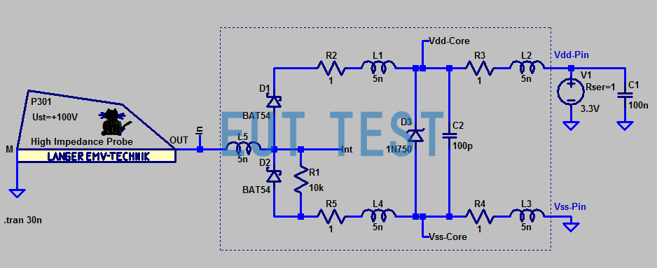
Fig. 9 Simplified LTSpice model of the high impedance probe P301 at the input of the IC equivalent circuit
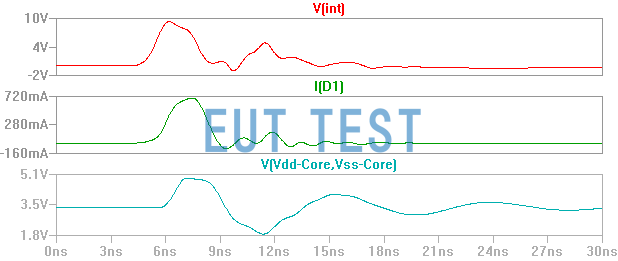
Fig. 10 Curve shapes for LTSpice simulation using high impedance probe P301
For a test voltage of +100 V, an interference voltage V(int) is generated in the IC. The current I(D1) flows through the protection diode D1. currently reloads the core capacity. Inside the IC, a transient response occurs on the power system V(Vdd-Core, Vss-Core) (Figure 10The core voltage drops from 3.3 V to 1.8 V and may cause the IC to fail.) In this case, the core voltage drops from 3.3 V to 1.8 V and may cause the IC to fail.
existFigure 11The LTSpice model of low impedance Probe P201 is connected to the Vdd pin of the IC equivalent circuit. Spare capacitor C1 has been removed and replaced with Probe P210. a voltage of -10 V has been applied to Probe P201. Interference produces a -4 V drop across the Vdd pin (Figure 12). The interference current flows to Vss mainly through the power clamp D3 and core capacitor C2. when this happens, the core voltage V(Vdd-Core, Vss-Core) drops to -1.2 V. This definitely interferes with the function of the IC.
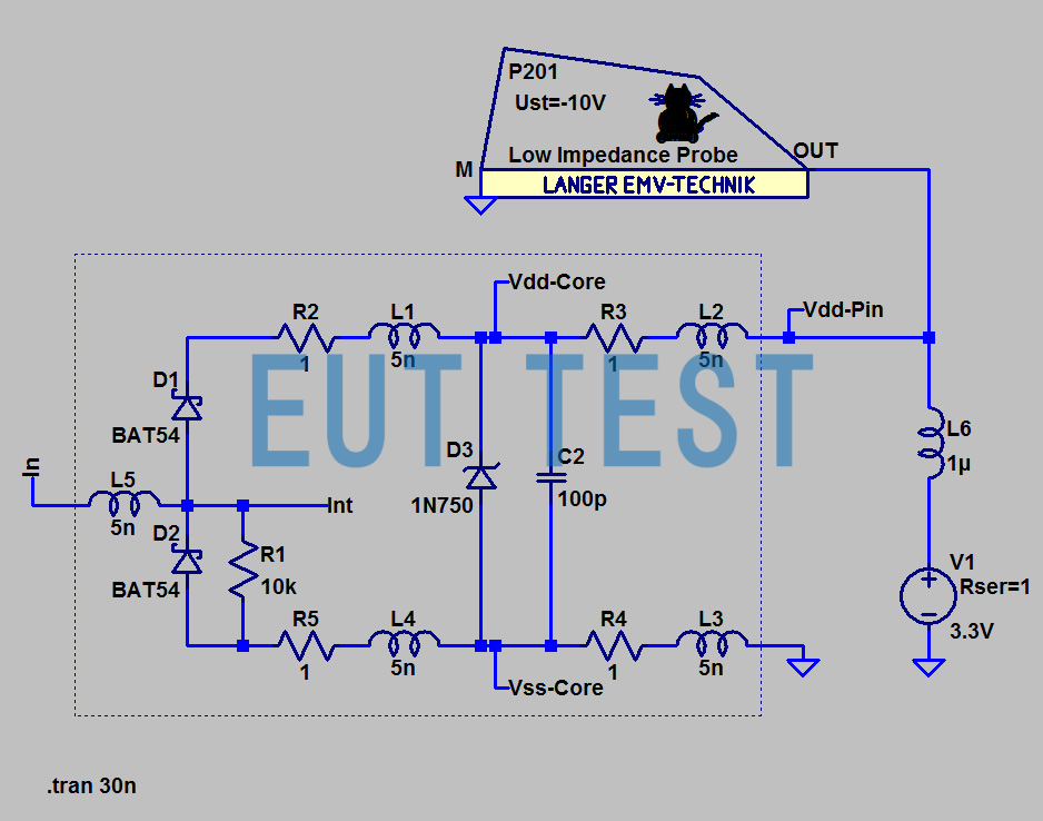
Fig. 11 Simplified LTSpice model of the low-impedance probe P201 at the input of the IC equivalent circuit
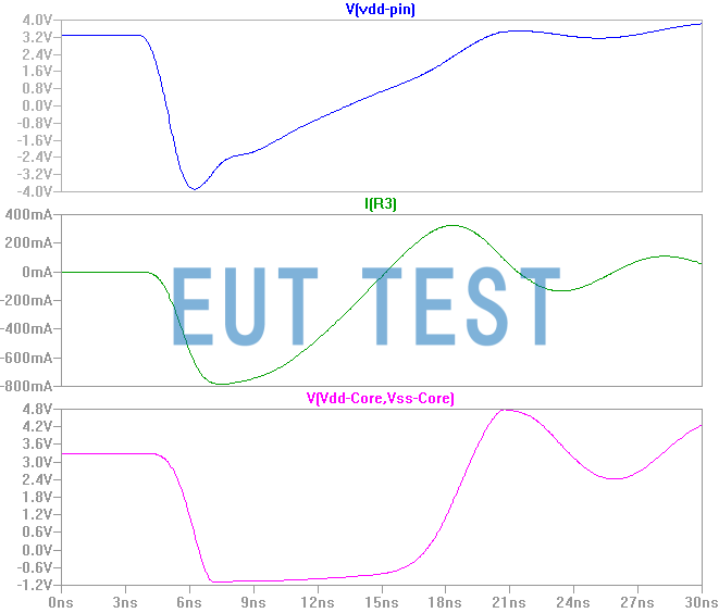
Fig. 12 Curve shape for LTSpice simulation using low impedance probe P301
Figure 11respond in singing12The phenomena shown are only exemplary to illustrate the IC process. Thus, a problem-solving approach for understanding highly complex disturbances in ICs is demonstrated.
By combining LTSpice simulations and tests with real ICs and probes (P201 and P301), the EMC characteristics of ICs can be studied and improved using efficient development tools. The LTSpice model of the test generator makes it easier for IC manufacturers to use the test programs described. In the future, one should be able to specify EMC properties at the beginning of IC development.