
IC EMC Sources of EMC problems in integrated circuits:
The number of mobile devices such as smartphones, tablets and wearables has increased significantly over the past few years. At the same time, wireless communication has increased due to higher data rates. Will the growing number of wireless devices increase EMC issues? Will today's industry be able to meet the EMC requirements that the IoT prepares us for?
If more devices have to interact with each other while their EMC quality remains at the current level, this will lead to more EMC problems from a statistical point of view. In addition, devices may be incompatible in practice even if they have passed conformance testing. For example, suppose that the electronic equipment has passed the emission compliance tests of IEC 61000-6-3, IEC 61000-6-4. Contrary to the tests, in practice the electronic equipment may be located near metal objects (e.g., enclosures). This can lead to field coupling, which in turn leads to higher emissions than in the tests. In this case, the size of the metal object is essential. The field may excite standing waves appropriate to the size of the metal object, which then leads to additional emission.
This means that in the future, there will not only be problems with wireless transmission, but also with device radiation.
Stricter device standards won't necessarily solve this compatibility problem.
The above example shows that current conformance tests typically do not consider any field coupling mechanisms. Field coupling mechanisms may trigger some useful ideas on how to solve the problem.
Nowadays EMC test standards for IC integrated circuits:
It remains to be seen whether the measurement principles set out in the current standards are sufficient or whether new measurement principles need to be developed.
In addition, new requirements have emerged in the field of EMC standards for ICs (IEC 61967 and IEC 62132). In the future, specific IC EMC parameters will be required as input values for EMC development tools/PCB simulation programs. It is advisable to obtain these EMC parameters from measurements according to the IC EMC standard. Unfortunately, the results of current standard measurements are not sufficient for this purpose.
This program will become even more important in future IC development.
This is why consideration should be given to adapting test methods for standard measurements to this task. This will be illustrated in the following by using conducted emissions as an example for ICs.
Current interference suppression strategies used in electronics development encounter their limitations. ICs that are potential sources of emissions are not considered troublemakers until the first development sample is completed. Developers encounter them when taking interference suppression measures on devices or PCBs. Near-field probes are used to locate RF sources in electronic devices. These do not recognize the IC itself as a source of interference, but rather feed the IC into the PCB alignment where the interference currents and voltages are. The electronics will then be modified with add-ons, copper foils, or other means. Last but not least, EMC measurements are performed to confirm the success of the interference suppression measures taken after the PCB redesign.
This approach is very time consuming and expensive. A big problem here is that selective EMC measures cannot be taken until the first sample of functional development is completed. Gain EMC critical insight when it is too late. Important decisions are made in the development process without considering the results of EMC testing. Problems are almost inevitable because EMC test results are obtained at such a relatively late point in time.
However, the industry needs faster, more efficient development that is compliant with EMC. This can only be achieved by adopting a completely new approach. This must start early in the development process and delve deeper into the action chain of emissions. Only the knowledge of actually operating the emission sources will allow developers to follow this path. Once ICs have been more accurately characterized as potential sources of emissions, appropriate measures can be taken earlier and more efficiently to stabilize the EMC of the entire device.
Appropriate EMC parameters are a prerequisite and therefore highly demanded. They must describe the EMC problem areas of the ICs for practical use in industry, which means that they must be suitable for the development of EMC-compliant PCBs. This means that they must be suitable for the development of EMC-compliant PCBs. in addition, the EMC parameters of the ICs must be linked to practical measures and strategies.
This approach should define electronics development in terms of EMC. Due to extreme miniaturization, the field of device development today is more sensitive to electromagnetic interference. Equipment manufacturers are increasing their efforts to address these issues in order to suppress interference in equipment and comply with appropriate standards.
The problems described in the example above exacerbate the situation. A key requirement of the IoT is that devices operate properly and reliably in their environment.
It remains to be seen to what extent equipment manufacturers will be able to continue to take control of the EMC situation that has worsened as a result of miniaturization and to curb interference in their equipment by spending more time and money on this task. EMC-compliant development will account for an increasing share of device development costs, and it is doubtful that EMC goals will be fully realized. This problem can be mitigated by providing better EMC parameters in future IC research and IC development. However, this means that more time and money must be spent here as well. This, of course, relates to wireless devices. The German industry has already begun to cope with this increasing pressure.
The company is now working with EMC consultants to use new EMC technologies to address EMC-related issues in the development of equipment and complex systems from the very beginning of the development process.
EMC Electromagnetic Compatibility Coupling Mechanisms within IC Integrated Circuits
ICs generate RF voltages, currents and fields due to internal functional operations. Different physical mechanisms are responsible for these entering the cable harness in the form of emissions or entering the surrounding open space in the form of radiation.ICs may have the following effects:
Conductive: emits RF current and voltage into the PCB traces through the IC pins.
Capacitance/Inductance: emits E and H near-field from a chip or IC connection.
Radiation: Direct emission of electromagnetic waves. For ICs with very high clock frequencies in practice, direct emission is usually only critical in the gigahertz range.
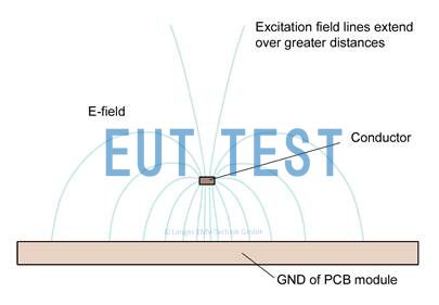
Fig. 1 Electric field of PCB alignment
The following section describes theItems 1 and 2: Conductive, capacitive and inductive effects in PCBs.
The emissions follow a closed loop. The driving RF current and RF voltage sources are located inside the IC. They drive the RF through bonding wires, leadframes, and pins into the PCB trace, where the current generates the near magnetic field and the voltage generates the near electric field. If the PCB trace is freely oriented in space, the electric and magnetic near-fields are established without interference. These fields are similar to the E-field and H-field of an antenna. The electric field passes through the antenna elements, whose currents and voltages are tightly coupled to the magnetic field. This electric field pattern results in the emission of electromagnetic waves. the PCB traces act as transmission antennas.
However, the situation on a PCB is often quite different. the PCB contains metal surfaces. These metal surfaces typically extend across the PCB and have a ground or supply voltage potential. The gap between these metal surfaces and the PCB trace is typically less than 1 mm. These grounded surfaces affect the distribution of electromagnetic fields along the alignment. This effect can best be described using the example of a loop antenna. If placed freely in space, a loop antenna can emit electromagnetic radiation. If the loop antenna is placed on the ground, this will prevent the emission of electromagnetic radiation. This is because the corresponding conductive metal surface will block the magnetic field at the loop opening, which is responsible for the current/field displacement effect (skin effect). The loop antenna' s magnetic field is no longer built up around the antenna and practically no longer exists. As a result, the radiated emission from the loop antenna is greatly reduced (Figure 2).
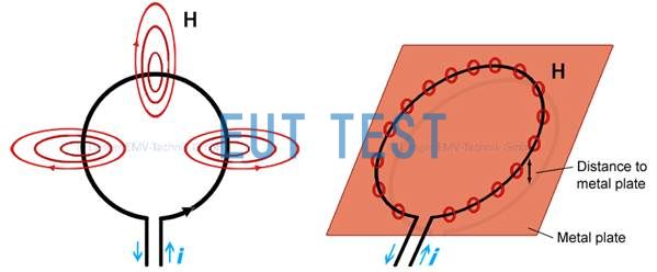
Fig. 2 Blocking the magnetic field of a loop antenna with a metal plate.
When the magnetic field is blocked, the near field of the loop antenna can stimulate the metal plate to radiate emissions (other radiation properties). If the gap between the loop antenna and the metal plate is zero, the H field is also zero.
PCB alignments react in exactly the same way. Once the ground surface in the PCB is large enough, direct radiation from the alignment is prevented. The emission from the alignment does not increase until a certain distance from the ground is reached. The required distance depends on the length of the alignment. Practical experience shows that the gap must be > 0.5 cm to cause any effective emission (frequency range 10 cm.
This means that PCBs are emitted in other ways, i.e. through their near field.
These near-fields cause emission by interacting with metallic components (Vdd/Vss surfaces, large metal parts, cables and wiring, metallic structural components).
Relationship between IC Voltage and Emission
In the following we refer to the PCB alignment. the internal IC alignment follows the same principles. Therefore, statements on the PCB alignment can be transferred to the internal IC alignment, and pin voltages on the PCB alignment or the internal IC alignment create an electric field around that alignment (Figure 1). Most of the field lines lead to the GND surface of the PCB. Only a few field lines leave the PCB vertically and penetrate into open space. The closer the alignment is to the edge of the GND system, the more field lines pass through the space.
These field lines (excitation field lines) leave the GND system of the PCB and transmit displacement currents through space, which stimulate electrical vibrations throughout the metallic system (PCB with cables and metal structural components).Figure 3).
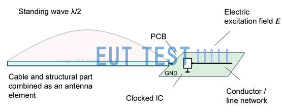
Fig. 3 Stimulation of radiant emission by electrically excited field lines
Standing waves on metallic systems may cause emissions.
The electrical excitation field can reach the metal parts located on the opposite side of the PCB (cables, structural components, shielding plates, etc.).Figure 4), and these components may be excited by the transferred displacement current to produce electrical vibrations.
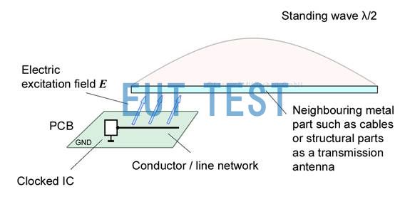
Fig. 4 Overcoupling of excitation field lines with neighboring metal parts
Relationship between IC current and emission
The current loops of an IC can be located inside the chip or formed by the pins of the IC. These loops run through the PCB, pins, leadframes, solder wires, and the grounding system of the chip. For example, this type of loop can be formed through the Vdd or Vss pins. Vdd / Vss loops that penetrate to the outside can be much larger than those located inside the chip. Larger external loops can generate stronger magnetic fields and are usually responsible for the highest emissions.
In the following we refer to the PCB alignment. the internal IC alignment follows the same principle.
As a result, declarations on PCB alignments can be transferred to alignments inside the IC.
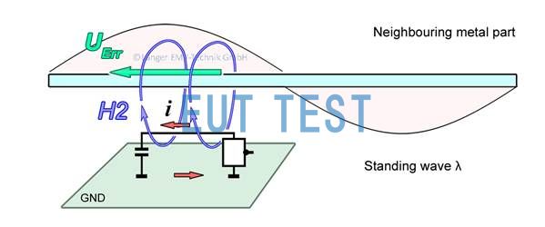
Fig. 5 Stimulation of radiant emission by mutual induction
Pin currents flowing into the PCB traces establish the magnetic field H2 (Figure 5). The return pin current also generates a magnetic field H1 in the GND system (Figure 6). It is assumed that the PCB ground is a metal surface that extends over the entire PCB. The alignment is very close to the ground and usually produces only negligible emissions, as in the loop antenna example above. The field H1 of the return current induces a self-sensing voltage U Err. The GND plane (metal surface) on the PCB. This voltage drives the cable and the structural components connected to it, such as antennas. As a result, the cable and structural components emit electromagnetic waves.
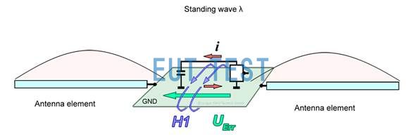
Fig. 6 Stimulation of radiant emission by mutual induction
The magnetic field of the trace H2 (Figure 5) does not produce any radiation in an open space. This is because the alignment is close to the ground plane, similar to the loop antenna example above, thus preventing radiation. There is another chain of interactions that can cause magnetic field radiation to be emitted. This is similar to that described above for field H1. For this purpose, metal parts must be inserted into field H2. If the magnetic field surrounds the metal part, an excitation voltage is induced there only by mutual induction. The excitation voltage stimulates the metal part to act as an antenna. The metal part emits electromagnetic waves. Take, for example, a steering column, a metal pillar or a cable near a PCB in a car.
EMC Parameters for IC Pins
IC pin currents and IC pin voltages are the IC pin-related EMC parameters. the electrical and magnetic near-fields of the IC are the field-related EMC parameters of the IC. all four parameters (u, i, E, and H) of the IC have to be detected by suitable measurement equipment.
The electrical near-field of the PCB alignment is proportional to the pin voltage, and the magnetic near-field of the PCB conductor loop is proportional to the pin current of the IC. The pin currents and pin voltages depend on the loads that the pins are subjected to through the connected PCB traces.
The IC parameters must use the values for the case that produces the highest pin voltage and the highest pin current.
The current and voltage of the alignment depends on the drive voltage in the IC and the impedance of the load on the PCB alignment.
If the pin is operating in a short circuit condition, the maximum possible pin current is measured. If the pin is operated under no-load conditions (open circuit), the maximum possible pin voltage is measured. Thus, the maximum possible value has been determined and all values in practice (determined in a large number of measurements on different PCBs) are equal or smaller.
In particular, PCB alignments have the highest voltage and electrical near-field under open circuit conditions. Then the emission potential is highest.
The corresponding EMC parameter for this IC is its open-circuit voltage Uliter(F).
The magnetic field near field is proportional to the current flowing through the trace. The current depends on the drive voltage of the IC and the load on the trace. In special cases a short circuit may occur. The current, the magnetic field and the resulting emissions are maximized.
The EMC parameter corresponding to IC is its short-circuit current I k (f).
Maximum pin current and pin voltage values (U l (f), I k (f)) are generated in the case of shorted or open pins. In these cases, the highest emissions are generated by the coupling mechanism described above.
Therefore, each pin of the IC has its own EMC parameter for conducted emissions.The EMC parameters for the IC pins are their open-circuit voltage and short-circuit current.
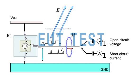
Figure 7 Pin parameter measurements close to short-circuit and open-circuit conditions
The open-circuit voltages and short-circuit currents for most of the pins of the IC can be determined from measurements taken under near open-circuit and short-circuit conditions. For example, two spectra per pin result in 128 spectra for a 64-pin IC. In addition, pins can have different switching states (input, output H, L, and high impedance). Internal functions can also have different states (Clk-PLL OFF/ON).
The current in the power supply pins is measured according to the 1 ohm method. If 1 ohm is too large, a 0.1 ohm measurement resistor is used. This measurement can be performed in Vdd and Vss. Corresponding high impedance probes and decoupling capacitors can be used to measure the RF open circuit voltage on the crystal oscillator pins. The filter capacitors of the crystal oscillator can be used as decoupling capacitors.
Measurements can generate large amounts of data and become difficult to manage. 3D representations provide a clear overview of the results (Figure 8). A custom-developed measurement setup with corresponding software (ChipScan ESA) allows semi-automatic recording of needle spectra. The results are displayed in 3D. For selected pins, the representation can be switched to 2D (Figure 12).
Use of IC parameters
The 3D spectrum clearly reveals problematic pins in practical applications. open-circuit voltages in the 80 dBµV range result in more than about 10 mm (especially problematic in automobiles). The critical frequency range can be read from the 3D - 2D spectrum.Figure 12Crystal oscillator pin 15 shows this. the critical frequency range is extended to 600 MHz. The critical frequency range extends to 600 MHz. it is possible to save time and money by orienting the layout and design in the right direction according to the EMC parameters of the IC pins. In some ICs, individual pins show high values for the conducted EMC parameters of emissions. These values provide useful advice on how to use the ICs on the PCB in a compatible way. Therefore, it is not necessary to exclude these ICs from development; IC users should determine the EMC parameters of the ICs before starting PCB development.
If the IC is integrated without this information (as is still common practice today), problems do not arise until the first development samples are measured. This leads to high costs for time-consuming interference suppression measures (layout changes, design modifications, etc.). This approach also allows the IC to be selected from a range of alternatives, as it is likely to result in lower emissions, and therefore making its PCB components EMC-compliant is easier and less costly.
Two new useful tools can be created for electronic development based on the EMC parameters of the IC:
Pin-dependent open-circuit voltage and short-circuit current spectra (3D / 2D)
Layout and Design Tips and EMC Parameters for IC Pins
EMC specialists can derive such design tips (countermeasures) from pin spectra, interactions (items 1 and 2), and characterization of particular applications. However, in practice, it is best to provide design hints and tips in the form of pin information.IC Pin EMC Parameters U l (f), I k (f) Frequency-dependent levels can be grouped into ranges with different risk potentials. Certain design measure barriers must be established based on the potential risks. This strategy will form the basis for EMC's activities in the coming years.
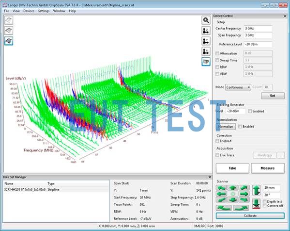
Figure 8 Testing the open-circuit voltage of IC 01
Example of pin-selective countermeasures in terms of open-circuit voltage:
Figure 8Static port pins 16 through 35 show high open-circuit voltage. If multiple port conductors are connected to the PCB trace, this can lead to emissions through the electric field. As a countermeasure, the alignment should be well surrounded by GND and not located at the edge of the PCB.
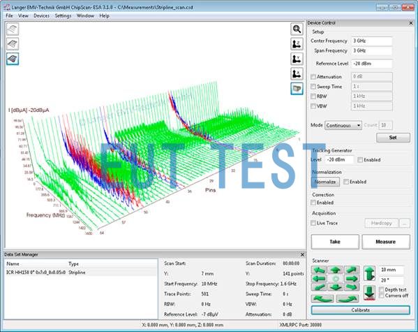
Fig. 9 Testing the short-circuit current of IC 01
Example of pin-selective countermeasures for short-circuit current
Port pins 16 through 35 also provide relatively high short-circuit values (Figure 9). Filter capacitors located far away from the IC can create a critical current loop. As a countermeasure, the filter capacitor should be located near the IC or a series resistor should be inserted.
High values are obtained in the lower frequency range (< 100 MHz) for power supply pins 12, 13 and in the mid-frequency range (approx. 500 MHz) for pins 50, 51, 52. As a countermeasure, resistors ( 20 mm). ICs should be positioned so that the IC current loop is orthogonal to the longest axis of the PCB. This is especially true for PCBs up to 50 mm wide. The direction of the IC current loop can be measured with a field probe designed for RF field measurements on ICs and provided as an IC EMC field parameter.
IC pin EMC parameter measurement system
Figure 10Shows the measurement settings for pin current and pin voltage measurements.
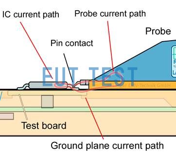
Figure 10 Measurement system for pin current and pin voltage
The test IC (DUT) is placed on a test board embedded in a ground plane. This provides a continuous GND surface as a prerequisite for measurements up to the GHz range.
A (voltage or current) measuring probe, whose tip can be easily moved to contact each pin, is placed on the GND plane. The measurement path (IC - pin contact - probe) is only a few millimeters long, so measurements can be made over short electrical distances.The IC is powered and controlled by the connection board through a filter (Figure 10). Connection plate integrated in the ground plane
IC EMC test case study
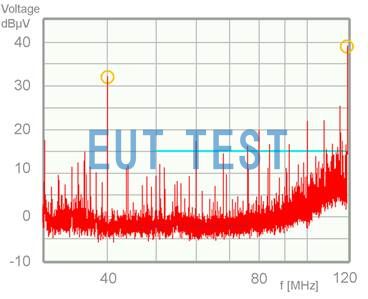
Figure 11 Measuring IC 02 Applications Using Analog Onboard Power Systems
The limit of 24 dB at 120 MHz is exceeded. Cause: Electric field coupling out of the trace connected to IC 02.
Figure 11Measurements of vehicle components were summarized. A limit violation of 24 dB at 120 MHz occurred due to the E-field. This problem was not discovered until after the development of the prototype test. The open-circuit voltage of the IC pin, one of the IC EMC parameters, U l (f) Measurements reveal why.
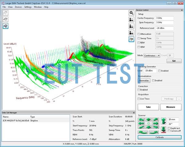
Figure 12 Open Circuit Voltage Measurement of IC 02 in 3D
Figure 12 Open Circuit Voltage Measurement of IC 02 in 2D
An unusually high voltage (about 80 dBµV at 120 MHz) was measured on the IC pin of the crystal oscillator in a 40 MHz grid (Figure 12(shown in black in the center).
All wiring and metal parts connected to these pins emit electric fields, such as physical mechanisms1stThe following is an example of what is described in this section. Unusually strong electric fields can cause electrical vibrations in the PCB and harness.
This implies that the field is coupled via:
The solder lines and lead frames that lead to the IC pins of the crystal.
15 mm PCB run from IC to crystal oscillator.
Crystal Oscillator Housing and Crystal Oscillator Wiring 3 x 0603 SMD Assemblies.
A suitable remedy in this case would be to reduce the surface of these metal parts, i.e., shorten the alignment and embed them in the GND to use a smaller crystal oscillator housing. However, in our example, these countermeasures are not sufficient. The open-circuit voltage of the pin U l (f) So high that the metal surfaces of the bonding wires and leadframes are large enough to cause the limits to be exceeded during component measurements. Filter capacitors cannot be used to reduce the voltage on the crystal oscillator. An electric field shield directly above the IC can be used as a last resort.Figure 13Shows positive results as a result of these responses. Limit values were met.
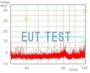
Fig. 13 Verification measurement after countermeasures: IC 02 Shielding prevents electric field coupling output.
Today it is possible to determine the EMC characteristics of an IC. It is useful if the values obtained are entered in the product data sheet. This information allows developers to plan the EMC measures required for the PCB already during the development process, so that they can in principle use any IC.
Test methods for determining IC EMC parameters enable IC manufacturers to develop ICs more efficiently.
Due to the continuous miniaturization of modules and the large number of very complex electronic devices, the EMC evaluation of ICs is an important prerequisite for the future development of electronic devices.
The use of IC EMC parameters will also have a positive impact on the development of IoT