
Introduction:
Electromagnetic simulation is a method of usingEM simulation and analysis softwareModern methods for analyzing the performance of electronic devices and systems are one of the core technologies in the modern field of electronic design automation (EDA) It replaces expensive and time-consuming traditional manual prototyping. To accelerate the design process and meet tight delivery schedules, engineers need to be able to perform cross-structural and multi-physical field analyses to model, simulate, and analyze the impact of these on system-level designs.
Ingredients:
Electromagnetic simulation software is divided into two parts: circuit simulators and field simulators. Electromagnetic field simulation software is categorized according to frequency criteria; static electric and magnetic field simulation software is used for low frequencies, and electromagnetic software is used for high frequencies. The more popular field simulation methods include finite element method (FEM), boundary element method, finite difference method, transmission line matrix method, and method of moments.
EM simulators first obtain a physical description of the device and then process the layout into a form that can be used in the analysis phase. This usually involves "meshing" the conductor using the Finite Element Method (FEM). A system of Maxwell's equations based on electromagnetism is analyzed and the solutions are combined to give the final result. The results of the analysis are provided as a model (e.g. S-parameters) which can be used in circuit simulation to verify performance.
The Importance of EM Electromagnetic Simulation
Today's high-performance electronic systems are being driven by increasing complexity and density, requiring designers to consider electromagnetic interference (EMI) and electromagnetic compatibility (EMC) as well as power integrity (PI) and signal integrity (SI) issues.
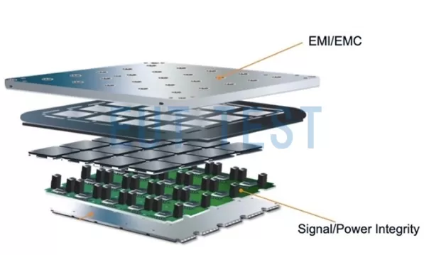
EMC and signal integrity problems in electronic systems
To accelerate the design process and meet tight delivery schedules, engineers need to be able to perform cross-structural and multi-physics field analyses to model, simulate, and analyze the impact of these on system-level designs.
The two main reasons for performing EM simulation are to discover any unintended EM interactions in a circuit/system and to ensure that the design meets the performance specification. In addition, designers need to perform EM simulation in different situations, such as when designing a chip, package, board, or system, to optimize the current design by looking at the simulation results and then tweaking it for further improvement. Alternatively, EM simulation is useful in the acceptance phase after the design is complete, and it is important to confirm that the design is fully optimized and meets the specification.
Where EM simulation can be used
Electromagnetic simulation and analysis in design
Electronic product development projects traditionally include a workflow where detailed multi-physics field EM simulation, analysis and optimization occurs in the later stages of the design process, often as the final step in verification and sign-off. However, such delays inevitably lead to costly issues that can derail budgets and delay time to market as requirements and performance flaws are discovered and additional cycles are required to address them. These issues should be identified and mitigated early in the design phase.
To succeed in today's competitive electronics market, multi-physics EM simulation and analysis is now being integrated from the earliest stages of the design process into a methodology known as "In Design Analysis (IDA)" that is moving from an afterthought in the workflow to an integral part of each stage of the design process at the chip, package, board, and complete system level. It is being transformed from an afterthought in the workflow to an integral part of every stage of the chip, package, board and complete system-level design process.
RF/microwave analysis in design
The RF/microwave device design workflow provides EM optimization, parameterization, 3D EM libraries, circuit co-design, full-wave EM extraction, and multi-structured EM hierarchy support.RF EM design-in technology allows design teams to transition from ideal circuit design to physical design with EM-level accuracy, building more complex circuits in a very logical and prescriptive way, helping them to achieve their goals in the fastest time possible. achieve their goals.
The 3D FEM solver can be used in the early stages of RF design, component EM modeling, circuit extraction, and optimization to identify problems before they occur in the prototype stage. These features include 3D EM parametric component and model libraries, support for hierarchical EM analysis of heterogeneous designs, and EM on-demand extraction capabilities.
Analysis in automotive electronics design
Every industry is expanding to embrace electrification, including mobile's communications, aerospace/defense, industrial, biomedical and consumer. Notably, the modern automobile is expanding to include increasingly sophisticated electronics, and manufacturers are equipping their new models with advanced driver assistance system (ADAS) applications that reduce injuries and fatalities by alerting drivers and assisting them with a variety of issues, including collision avoidance and low tire pressure, as well as automated parking and driving. These systems are becoming increasingly complex as the demand for functionality increases, making EM simulation and analysis in design critical to delivering reliable and superior performance within a shrinking market window.
Analysis in the design of high-speed devices
In critical electronics applications such as high performance computing (HPC), automotive, machine learning, and 5G, data speeds and volumes are growing exponentially. Crosstalk analysis and simulation in high-speed designs is difficult without the right field solving tools or analytical models. Designers of modern high-speed PCBs need to consider single-ended and differential crosstalk that can be mistaken for crosstalk, as well as power integrity issues.
Designers need field EM analysis to understand the relationship between physical design and overall system performance. Combined with integrated EM simulation and multiphysics field analysis during the design process, engineers also need solutions that enable a complete and comprehensive high-speed and high-frequency design and analysis workflow within a single platform that extends beyond the chip and into the entire system.
In order to meet these requirements.EMI/EMCand SI/PI techniques can be used throughout the design process to quickly and accurately process the largest and most complex structures, identify crosstalk-susceptible interconnections, and take steps to prevent noise coupling between interconnects.
 EMC test analysis from device to chip